My side of an argument with Jacob Cannell about chip interconnect losses
Context / How I came to write this
Jacob Cannell (@jacob_cannell) made some claims about fundamental limits of interconnect losses on chips at Brain Efficiency: Much More Than You Wanted To Know, and in particular claimed that current chips have interconnect losses close to as low as they will ever get.
When I read that claim I thought it was wrong, as was Jacob’s discussion of interconnect losses more generally, but I didn’t (and still don’t) think the disagreement directly mattered for AI x-risk, so I mostly didn’t want to spend time arguing about it.
But then later Alexander Gietelink Oldenziel wrote $250 prize for checking Jake Cannell’s Brain Efficiency, and I wound up in a 15-comment back-and-forth with Jacob about it, before ducking out. (Other people continued that thread afterwards).
Unfortunately, I quit the discussion while still being confused about where Jacob was coming from. So this post will not be maximally good and useful, sorry. Nevertheless, here’s a summary of my current perspective and understanding, in case anyone cares.
Also see comments section at the bottom for a response by Jacob.
(Jargon level: medium-low maybe? There is still some unexplained physics & EE jargon, but hopefully I made the centrally important parts accessible to non-experts. DM or email me if something is confusing, and I will try to fix it.)
(All numbers in this post should be treated as Fermi estimates.)
(Thanks very much to Jacob for his extraordinary patience in trying to explain to me his perspective on this topic. And also his perspective on many other topics!)
Background to the technical disagreement
“Interconnects” send information from one point to another on a chip.
The fundamental thermodynamic limit for the power required to send a bit of information from point A to point B is 0.[1] As a stupid example, there is a lot of digital information on Earth, and it all travels meters in orbit around the sun each year for roughly zero energy cost.
Chip interconnect losses are obviously much much higher than the thermodynamic limit of “zero”—they might even constitute a majority of chip power consumption these days. Everyone knows that, and so does Jacob. So what is he saying?
I think Jacob divides the world of interconnects into two categories, “reversible” and “irreversible” interconnects, with the former including optical interconnects and superconducting wires, and the latter including normal wires and brain axons. (I’m stating this categorization without endorsing it.)
I think Jacob takes “reversible” interconnects (optical interconnects & superconducting wires) to have a fundamental interconnect loss limit of zero, but to have practical limits such that we’re not expecting to cut orders of magnitude from the total interconnect loss budget this way. I agree with his conclusion here, although we had some disagreements in how we got there. But anyway, that’s off-topic for this post.
(See my brief discussion of optical interconnects here—basically, nobody seems to have even a roadmap to making optical interconnects with such low power that they could replace almost all (say, >90%) of the aggregate on-chip interconnect length.)
Instead our main dispute was about voltages-on-wires, the workhorse of within-chip communication. Pause for:
On-chip wire interconnects for dummies: As background, here is the oversimplified cartoon version of integrated circuits. There are a bunch of metal wires, and there are transistors that act as switches that connect or disconnect pairs of wires from each other. Depending on which transistors are “on” versus “off” at any given time, any given wire may wind up connected to one of two possible fixed-voltage sources (either “ground” = 0 mV, or so-called “” ≈ 500 mV).[2] Once any part of that wire is contacting one of those sources, the entire wire (being conductive) winds up at that specified voltage level. And meanwhile a different part of that same wire is connected to the “gate” of one or more transistors, and depending on the wire voltage, that transistor might switch “on” or “off” in turn, which can change the voltage of still other wires, and so on forever. Thus, the wire is a mode of information transmission: one side gets set to a certain voltage, and then that same voltage value can be read off at the other side, which might be quite far away.
Jacob believes that there is a certain fundamental limit on interconnect losses when we transmit information via voltages on wires—something in the neighborhood of , which he claims is not terribly far from what it is in modern chips (I didn’t check that part). I think he’s wrong that this is a fundamental limit.
My model: Why 6 orders of magnitude (OOM) reduction in on-chip interconnect losses is very hard but not impossible
Credit for this way of thinking goes to UC Berkeley professor Eli Yablonovitch (any errors are my own). See for example this 2012 talk with the basic idea, or this 2019 talk with more on implementation concepts & prototypes. By the way, this basic idea is the guiding philosophy of the Center For Energy Efficient Electronics Science, a center Yablonovitch directs, which got $50M of US-NSF funding over 10 years.[3]
My model centers around the following major issue:
The easiest way to reliably actuate a switch is with a voltage of at least 500 mV, corresponding to a voltage high enough to use normal transistors as the switches,[4] as opposed to the weirder approaches in the Appendix. (kT is defined at this link, q is the elementary charge, and 20 is a factor that gets us way above the noise floor.)
The most energy-efficient way to reliably send information down a wire is to use a voltage around 0.7 mV, where 20 is a factor that gets us way above the noise floor, f is the frequency bandwidth of the noise that we care about (let’s say f ≈ 3 GHz for a chip), and Zeff is the wire’s effective impedance (looking towards the wire from the receiver), let’s say probably 50-100 Ω in practice.[5]
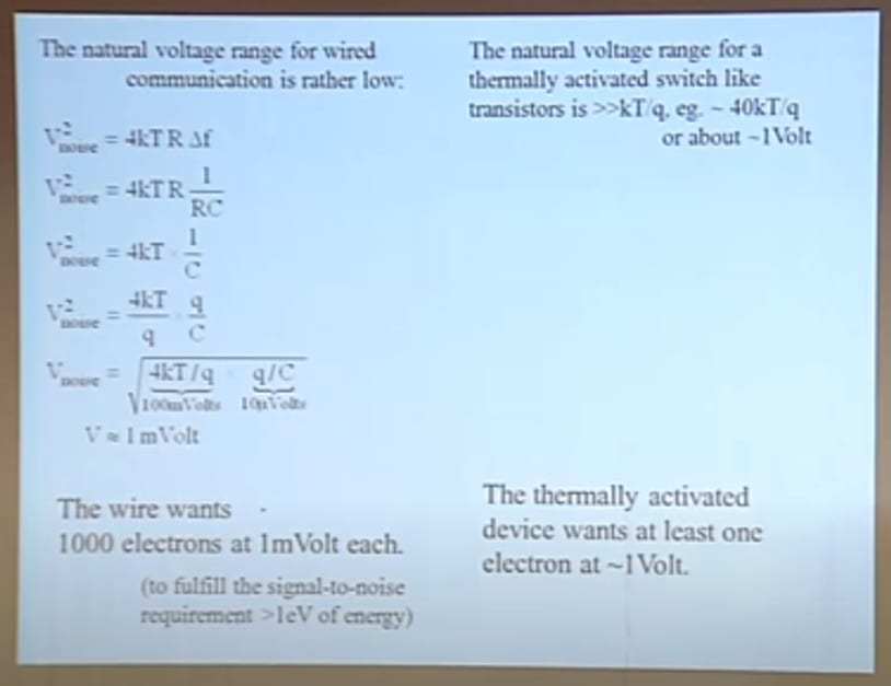
So there’s a giant (3 OOM) mismatch in what voltage makes sense.
The “easy way” versus the “hard way” to deal with that giant voltage mismatch
The easy way to deal with that giant mismatch is to ignore it. Just use the same 500 mV voltage for both the switches and the wires. Unfortunately, this method is horrifically bad for interconnect losses: the power required to send a bit down a wire increases quadratically with voltage. So if we use 3 OOM higher voltage than necessary for sending a bit of information down our wires, our interconnect losses are 6 OOM higher than necessary.
Why quadratic? There’s a (undesired / stray) capacitor, one of whose “plates” is the wire, and the other of whose “plates” is whatever conductive stuff is in the vicinity of that wire. When you switch the voltage between ground and , you need to charge or discharge that capacitor by flowing current in or out, which dissipates energy .[6]
The hard way to deal with that giant mismatch is to succeed at one of the challenging approaches discussed in the Appendix. Those approaches all work in principle (I claim), and in some cases there are even proof-of-principle lab demos. But getting them to work at scale, in actual fabs, in a way that’s compatible with every other part of the chip-production process, doesn’t impact the yield or chip cost, and so on—that’s quite a different matter. I’m not particularly holding my breath.
So, people are not currently doing it the “hard way”, instead they are doing it the “easy way”, and they always have been.
Fermi estimate of interconnect losses on the assumption that people continue doing things the “easy way”
Given that people are in fact doing it the “easy way”, we can do a fermi estimate of interconnect losses as follows. We have and [7] (where L = wire length and is the physical constant), and there’s a factor of ½ because we only need to charge or discharge the capacitor half of the time (i.e., only when a bit is different from the preceding bit). So we finally get a fermi-estimate:
which is not wildly different from Jacob’s supposed fundamental limit on wire interconnects mentioned at the top.
Why do I bring up this fermi estimate? Well, Jacob seems to have updated hard on the fact that his (supposed) fundamental limit is in the same ballpark as actual chips. If his model is totally wrong, doesn’t that seem a remarkable coincidence?? Well, I think his model is totally wrong, and I think that this is a remarkable coincidence, albeit much less remarkable than you might think thanks to the magic of dimensional analysis.
Anyway, given that background context, it seems highly relevant to note that my model predicts interconnect losses in that same ballpark as Jacob’s model, and in the same ballpark as actual chips, if we’re doing things the “easy way” (as opposed to doing the stuff in the Appendix), which, again, is how we make chips today, and always have.
Prospects for doing things “the hard way” in the future
Will people ever switch to doing it “the hard way”? (by following one of the approaches in the Appendix, or something else in that category.) Beats me, especially if we’re talking about what’s going to happen before AGI apocalypse / utopia. (And as I wrote at the top, I don’t think this post is relevant for AI x-risk.) I feel pretty strongly that at least some of the approaches in the Appendix are based on sound physics and have no fundamental blockers—and therefore that Jacob is wrong about his supposed fundamental limit on wire interconnect losses. But actually getting these approaches into commercial chips is another matter entirely—one where all kinds of things can go wrong (or be cost-prohibitive).
Jacob’s model
Everything above was my model. What about Jacob’s model? Well, I’m not going to even try to describe it in my own words, because I don’t understand it. Sorry! You can read the thread and citations therein.
Some ways that Jacob & I seem to be talking past each other
I will, however, point to some things that seem to be contributing to Jacob & me talking past each other, in my opinion.
Jacob likes to talk about detailed properties of the electrons in a metal wire (specifically, their de Broglie wavelength, mean free path, etc.), and I think those things cannot possibly be relevant here. I claim that once you know the resistance/length, capacitance/length, and inductance/length of a wire, you know everything there is to know about that wire’s electrical properties. All other information is screened off. For example, a metal wire can have a certain resistance-per-length by having a large number of mobile electrons with low mobility, or it could have the same resistance-per-length by having a smaller number of mobile electrons with higher mobility. And nobody cares which one it is—it just doesn’t matter in electronics.[8]
I want to talk about wire voltage profiles in terms of the “normal” wire / transmission line formulas (cf. telegrapher’s equations, characteristic impedance, etc.), and Jacob hasn’t been doing that AFAICT. I can derive all those wire-related formulas from first principles (ooh and check out my cool transmission line animations from my days as a wikipedia editor!), and I claim that those derivations are perfectly applicable in the context in question (nano-sized wire interconnects on chips), so I am pretty strongly averse to ignoring those formulas in favor of other things that don’t make sense to me.
Relatedly, I want to talk about voltage noise in terms of the “normal” electronics noise literature formulas, like Johnson noise, shot noise, crosstalk noise, etc., and Jacob hasn’t been doing that AFAICT. Again, I’m not taking these formulas on faith, I know their derivations from first principles, and I claim that they are applicable in the present context (nano-sized wire interconnects on chips) just like for any other wire. For example, the Johnson noise formula is actually the 1D version of Planck’s blackbody radiation equation—a deep and basic consequence of thermodynamics. Here I’m thinking here in particular of Jacob’s comment “it accumulates noise on the landauer scale at each nanoscale transmission step, and at the minimal landauer bit energy scale this noise rapidly collapses the bit representation (decays to noise) exponentially quickly”. I will remain highly skeptical of a claim like that unless I learn that it is derivable from the formulas for electrical noise on wires that I can find in the noise chapter of my electronics textbooks.
Jacob wants to describe wires as being made of small (≈1 nm) “tiles”, each of which is a different “bit”, with information flow down wires corresponding to dissipative bit-copying operations, and I reject that picture. For example, take a 100 μm long wire, on which signals propagate at a significant fraction of the speed of light. Now smoothly slew the voltage at one end of the wire from 0 to over the course of 0.1 ns. (In reality, the slew rate is indeed not infinite, but rather limited by transistor capacitance among other things.) Then, as you can check for yourself, the voltage across the entire wire will slew at the same rate at the same time. In other words, a movie of the voltage-vs-position curve on this 100 μm wire would look like a rising horizontal line, not a propagating wave. Now, recall where the Landauer limit comes from: bit-copy operations require kT of energy dissipation, because we go from four configurations (00,01,10,11) to two (00,11). The Second Law of Thermodynamics says we can’t reduce the number of microstates overall, so if the number of possible chip microstates goes down, we need to make up for it by increasing the temperature (and hence number of occupied microstates) elsewhere in the environment, i.e. we need to dissipate energy / dump heat. But in our hypothetical 100 μm long wire above, this analysis doesn’t apply! The different parts of the wire were never at different voltages in the first place, and therefore we never have to collapse more microstates into fewer.
…So anyway, I think our conversation had a bit of an unproductive dynamic where Jacob would explain why what I said cannot possibly be right [based on his “tiles” model], and then in turn I explain why what he said possibly be right [based on the formulas I like e.g. telegrapher’s equations], and then in turn Jacob would explain why that cannot possibly be right [based on his “tiles” model], and around and around we go.
Appendix: Some possible technical approaches to making “switches” on future ICs that are compatible with dramatically lower wire voltages than normal transistors are
Strategy 1: Just use normal transistors, but put nanoscale step-up voltage converters between the wires and the transistor gates that they connect to
Step-up voltage converters—which convert a low-impedance low-voltage source into a high-impedance high-voltage source—do not violate any laws of physics, and have no nonzero fundamental efficiency limit. If we could “just” put billions of tiny efficient 500:1 step-up voltage converters onto our chip, one for each transistor gate, then we could use , and goodbye 99.99%+ of interconnect losses.
But how do we make billions of tiny efficient step-up voltage converters?? I’m aware of a couple possible approaches.
Piezoelectric stacks: As I understand it, you can stack two nanofabricated mechanically-coupled piezoelectric blocks of different sizes, within a slightly-larger (but still nano-sized) stiff mechanical box. When you apply a voltage to one of the piezoelectric blocks, it turns into a strain, and that in turn applies stress to the other piezoelectric block, which induces a voltage. And depending on geometry and materials, you can arrange for the second voltage to be much larger than the first. See paper here (by a group at IBM). I endorse this approach as probably sound in principle. They seem to have abandoned the project, so I guess it probably has challenges in practice; I don’t know the details.
Ferroelectric “negative capacitance”: Under certain circumstances, a configuration of electrodes with ferroelectric materials can amplify voltages. I don’t remember the details, but I think I spent a few hours looking into it a decade ago and decided that the theory was probably sound. Work is ongoing I guess—here’s a random 2022 paper from this subfield.
Strategy 2: Find a different kind of switch that can switch at much lower voltage than transistors can, e.g. 1 mV
To be clear, the Landauer limit concerns the energy required to switch a switch, not the voltage required to switch a switch. So there’s no fundamental reason that a switch can’t work directly with much lower voltage.
Here are a few things in this field. All of these are drawn from this 2019 Eli Yablonovitch talk—see there for better explanations and references.
NEMS: You can “increase q” and thereby decrease . Wait, what? Recall, the electrostatic barrier is qV, where q is the electric charge of the thing climbing the barrier. In a transistor, the thing climbing the barrier is a single individual electron. But in principle one could develop a mechanical (NEMS) device that would switch a connection on and off the old-fashioned way—by actual physical contact between two conductors. The trick is that a mechanical cantilever could in principle have a charge of 10 e or 100 e or 1000 e or whatever (where e is the electron charge), and therefore a quite low voltage could actuate it without thermal noise being an issue. I’m sure there are issues with reliability, stiction, speed, and so on, but no fundamental barriers to my knowledge.
Tunnel FETs: Normal transistors work by using the voltage to raise or lower an energy barrier blocking current flow. But a different paradigm is that current flow is due to quantum tunneling, and the voltage is modifying the extent to which quantum tunneling is possible (it depends on aligned energy levels etc.). I’m not super confident that this works even in theory, but my guess is that it probably does work in theory. (As always, developing it to the point where it can be rolled out to chip fabs is another matter entirely.)
Spin-orbit torque: You can use an electrical current to switch the magnetization of a magnet via a phenomenon called “spin-orbit torque”. That magnetization can in turn change the resistance of an electrical connection via a different phenomenon called “magnetoresistance”. This setup apparently works, and is fast, but the on-off ratios are inadequate with currently-known magnetoresistance setups. On the other hand, there are numerous ways to get magnetoresistance, and I have no particular reason to believe that Science has discovered all of them already.
(Thanks again to Jacob for patience during that very long discussion, and sorry that I’m giving up without us reconciling. Thanks to Charlie Steiner for critical comments on a draft.)
- ^
OK, fine, I can imagine being convinced that there are inevitably up to 20 kT per bit (or whatever) that need to be dissipated for low-noise communication in certain circumstances, independent of interconnect length. But we can round that to zero—this post is talking about much larger amounts of energy than that.
- ^
Sometimes a wire will be in a “hi-Z” state, i.e. connected to neither of the two voltage sources, but that won’t matter for this post.
- ^
This whole footnote should be ignored by any readers willing and able to evaluate physics arguments on their merits. But other readers may be forced to rely on an Expert Credentials Pissing Contest, so this footnote exists to provide them with some relevant information. Here goes. I mentioned the NSF thing not because it is totally impossible for the NSF to have thrown $50M over 10 years at a set of projects that are fundamentally doomed on account of basic laws of physics, without anyone noticing. I do think that’s possible. But I think it’s pretty unlikely in this context. (And I say this despite generally thinking very little of the NSF’s competence.) At the very least, I think the NSF thing provides strong evidence that Eli Yablonovitch’s way of thinking has survived much much more expert physicist scrutiny than your average obscure peer-reviewed paper or two. Separately, I claim that Eli Yablonovitch in particular has a legible track record of being correct when he derives and/or popularizes conceptual insights based on basic physics principles. For example he was one of the inventors of the now-mainstream idea of “photonic bandgaps”, as well as the well-known “Yablonovitch limit” for light concentration in solar cells, among other things. While we’re at it, I can also list my own relevant credentials—physics PhD with extensive coursework in solid-state physics, semiconductor physics, semiconductor materials science, nanoelectronics, regular electronics, and thermodynamics, plus I’m listed on a transistor patent, albeit a pretty weird one, and one time I read a whole excruciatingly boring textbook on transistor noise… I can carry on if anyone cares to inquire in the comments.
- ^
A voltage of or so is required for normal transistors, and more broadly for any low-noise room-temperature switch whose mechanism involves (1) an energy barrier preventing current flow, and (2) a voltage V that raises or lowers this energy barrier by ±qV, where q is the elementary charge. The reason is as follows. Any switch in this category has the problem that the Boltzmann distribution enables some current flow even when the energy barrier is nonzero. This undesired current gradually cuts off as the energy barrier gets up to a sufficiently large multiple of kT. In the lingo, this problem manifests as the 60 mV/decade “thermionic limit” of “subthreshold slope” for transistors.
- ^
I think in the case of interest, Zeff is the same as the transmission line characteristic impedance, which tends to be 50-100 Ω. (This isn’t arbitrarily changeable—it’s pretty hard to get much above or below that for wires; it’s ultimately related to the 377 Ω impedance of free space, a fundamental constant of nature.) It’s not impossible AFAIK that the voltage source impedance is also relevant to Zeff, but that wouldn’t change the discussion here.
- ^
You may recall from freshman physics that the energy required to charge a capacitor is rather than like I said here. But squeezing out that extra ½ requires using a current source rather than a voltage source (or equivalently, ramping up the source voltage gradually as the capacitor charges up). That seems pretty unrealistic in the context of chips, I think, so I left out the ½. If I’m wrong, whatever, factors of 2 don’t really matter for this post anyway.
- ^
[THIS PART WAS EDITED JUNE 22] The formula for the stray capacitance of a wire is , where k is the dielectric constant of the so-called “interlayer dielectric” (maybe 2-3, or theoretically as low as 1 if you can use air-gaps between wires), and a is a unitless factor related to geometry, something like “how close together are the wires relative to their size”. There’s some discussion in the comments section here. According to that comments-section discussion, the lowest Intel can get in practice right now is . I used in the text to account for future technological development, and because it’s a nice round number. I can’t rule out that it will get even lower than 10 in the future, but this is just a fermi estimate anyway.
- ^
These parameters obviously matter to the person designing the wire, but once the wire is there, it stops mattering from an electronics perspective, I claim. Also note that semiconductors are very different from metals in that respect: Mobility and charge carrier concentration are independently centrally important in semiconductors, whereas only their product is important in metals. There is a good reason for this: namely, the number of charge carriers in a metal is so high that it cannot possibly noticeably change during operation, whereas the number of charge carriers in a semiconductor is sufficiently low that it can substantially jump around in real time during operation, for example via the field effect. OK fine, there are some cases where people care about the charge-carrier mobility in a metal, like in principle one could make a metallic Hall effect sensor, but the situation I’m discussing here is not one of those.
The picture from Eli Yablonovitch described here is basically right as far as I can tell, and Jacob Cannell’s comment here seems to straightforwardly state why his method gets a different answer [edit: that is, it is unphysical]:
[The rest of this comment has been edited for clarity; the comment by Steven Byrnes below is a reply to the original version that could be read as describing this as a quantitative problem with this model.] As bhauth points out in a reply, the atomic scale is a fraction of a nanometer and the mean free path in a normal metal is tens of nanometers. This is enough to tell us that in a metal, information is not “relayed through electrons exchanging orbitals”.
Valence electrons are not localized at the atomic scale in a conductor, which is part of why the free electron model is a good model while ignoring orbitals. The next step towards a quantum mechanical model (the nearly-free modification) considers the ionic lattice only in reciprocal space, since the electrons are delocalized across the entire metal. The de Broglie wavelength of an electron describes its wavefunction’s periodicity, not its extent. The mean free path is a semiclassical construct, and in any case does not provide a “cell” dimension across which information is exchanged.
The “tile”/cellular-automaton model comes from Cavin et al., “Science and Engineering Beyond Moore’s Law” (2012) and its references, particularly those by Cavin and Zhirnov, including Shankar et al. (2009) for a “detailed treatment”. As @spxtr says in a comment somewhere in the long thread, these papers are fine, but don’t mean what Jacob Cannell takes them to mean.
That detailed treatment does not describe energy demands of interconnects (the authors assume “no interconnections between devices” and say they plan to extend the model to include interconnect in the future). They propose the tiling framework for an end-of-scaling processor, in which the individual binary switches are as small and as densely packed as possible, such that both the switches and interconnects are tile-scale.
The argument they make in other references is that at this limit, the energy per tile is approximately the same for device and interconnect tiles. This is a simplifying assumption based on a separate calculation, which is based on the idea that the output of each switch fans out: the output bit needs to be copied to each of around 4 new inputs, requiring a minimum length of interconnect. They calculate how many electrons you need along the length of the fan-out interconnect to get >50% probability of finding an electron at each input. Then they calculate how much energy that requires, finding that it’s around the minimal switching energy times the number of interconnect tiles (e.g. Table 28.2 here).
For long/”communication” interconnects, they use the same “easy way” interconnect formula that Steven Byrnes uses above (next page after that table).
The confusion seems to be that Jacob Cannell interprets the energy per tile as a model of signal propagation, when it is a simplifying approximation that reproduces the results of a calculation in a model of signal fan-out in a maximally dense device.
I understand the second part of this comment to be saying that Jacob & I can reconcile based on the fact that the electron mean free path in metal wires is actually much larger than 1 nm. If that’s what you’re saying, then I disagree.
If the lowest possible interconnect loss is a small multiple of kT/(electron mean free path in the wire), then I claim it’s a coincidence. (I don’t think that premise is true anyway; I think they are off by like 4 OOM or something. I think there is like 6 OOM room for improvement in interconnect loss compared to Jacob’s model, so replacing 1 nm with copper mean free path = 40 nm in Jacob’s model is insufficient to get reconciliation.)
I think that, if there were two metal wires A & B, and wire A had 10× higher density of mobile electrons than B, each with 10× lower effective mass than B, but the electrons in A have 100× lower mean free path than B, then the resistivities of A & B would be the same, and in fact we would not be able to tell them apart at all, and in particular, their energy dissipation upon transmitting information would be the same.
One point of evidence, I claim, is that if I give you a metal wire, and don’t tell you what it’s made of, you will not be able to use normal electrical equipment to measure the electron mean free path for that wire. Whereas if the electron mean free path was intimately connected to electronic noise or binary data transmission or whatever, one might expect that such a measurement would be straightforward.
Oh, no. I just meant to highlight that it was a physically incorrect picture. Metallic conduction doesn’t remotely resemble the “electronic cellular automata” picture, any version of which would get the right answer only accidentally, I agree. A calculation based on information theory would only care about the length scale of signal attenuation.
Even for the purposes of the cellular model, the mean free path is about as unrelated to the positional extent of an electron wavefunction as is the de Broglie wavelength.
Firstly, part of the confusion here is my regrettable use of fundamental in the original article here:
But just after that I mentioned typical exceptions:
So I only meant ‘fundamental’ in the more narrow pareto tradeoff sense that if your interconnect is fully dissipative/reversible then the energy will be on around at least Eb/d where d is the distance scale of physical interconnect bits. For a macro scale domino computer, the distance scale is the size/spacing between dominoes. For electronic devices at maximum packing density where you naturally represent bits with single electrons, and the de broglie wavelength is then quite relevant as a constraint on maximum packing density due to quantum tunneling etc.
It’s also obviously energy inefficient to use nanoscale single electron bits for wires/interconnect—but that represents a core space vs energy tradeoff (amongst other optimization dimensions on the pareto surface). You can somewhat easily get much better wire energy efficiency by using much larger bit representations—like EM waves—but those are also much larger at 1eV energies.
One can also perhaps beat that bound by using anisotropic interconnect tiles where electrons move more ballistically as in some hypothetical carbon nanotube interconnect that could have a mean free path 3 OOM beyond copper[1] and proportionally lower bit energy per nm around perhaps 1e-22 J/bit/nm.
The aspect of this I consider fundemental is the more subtle notion of a pareto tradeoff surface around the landauer energy and nanometer scale, for dissipate nanoscale devices. The hypothetical CNT single electron interconnect tile device is fundamentally much slower than copper interconnect—as just one example.
Other interesting examples come from biology, such as kinesin, the motor walking protein, which can walk surprisingly large microvesicle ‘ballons’ down microtubules reliably using around an ATP per few nm—ie nearly the same natural energy bit scale. Typical microvesicles probably do not have a high bit information content, but if they were storing a large snippet of DNA that could increase the bits per unit distance at the same energy scale by OOM—but naturally at a cost of slower transmission.
Neural axon signal propagation has a bit energy scale tradeoff very similar to electronic devices, where the thinnest axons use around ~1eV/bit/nm (1e-19J/bit/nm), and the myelinated axons are a few OOM more efficient at around 5e-21J/nm or so[2], very similar to modern on-chip copper interconnect and coax cable wires (although meylinated axons are thinner at the same energy efficiency vs coax cable).
So I observe the fact that human engineering and biology have ended up on the same pareto surface for interconnect space & energy efficiency—despite being mostly unrelated optimization processes using very different materials—as evidence of a hard pareto surface rather than being mere coincidence.
Purewal, Meninder S. Electron transport in single-walled carbon nanotubes. Columbia University, 2008.
Derived from Ralph Merkle’s classic essay on brain limits.
Thanks for replying. This is a lot clearer to me than prior threads, although it also seems as though you’re walking back some of your stronger statements.
I think this is still not quite a correct picture. I agree with this:
However, at maximum packing density with single-electron switches, the energy requirements per area of interconnect space are still not related to dissipation, nor to irreversible-bit-erasure costs from sending signals tile by tile. Rather, the Cavin/Zhirnov argument is that the extra energy per area of interconnect should be viewed as necessary to overcome charge shot noise in the bit-copy operations required by fan-out after each switch. Abstractly, you need to pay the Landauer energy per copy operation, and you happen to use a couple interconnect tiles for every new input you’re copying the switch output to. Physically, longer interconnect reduces signal-to-noise ratio per electron because a single electron’s wavefunction is spread across the interconnect, and so is less likely to be counted at any one tile in the interconnect.
Thinking of this as accumulating noise on the Landauer scale at each nanoscale transmission step will give incorrect results in other contexts. For example, this isn’t a cost per length for end-to-end communication via something other than spreading an electron across the entire interconnect. If you have a long interconnect or coaxial cable, you’ll signal using voltage transmitted at the speed of light over conduction electrons, and then you can just think in terms of resistance and capacitance per unit length and so on. And because you need 1V at the output, present devices signal using 1V even though 1mV would overcome voltage noise in the wire. This is the kind of interconnect people are mostly talking about when they talk about reducing interconnect power consumption.
Thanks a ton for writing this, Steve! It’s immensely helpful for us laymen trying to follow along.
I look forward to Jake’s response.
This is an excellent writeup.
Minor nit, your assertion of C=ϵ0L is too simple imo, even for a Fermi estimate. At the very least, include a factor of 4 for the dielectric constant of SiO2, and iirc in real interconnects there is a relatively high “minimum” from fringing fields. I can try to find a source for that later tonight, but I would expect it ends up significantly more than 10×ϵ0. This will actually make your estimate agree even better with Jacob’s.
This page suggests that people have stopped using SiO2 as the “interlayer dielectric” in favor of (slightly) lower-dielectric constant materials, and also that Intel has a process for using air gaps for at least some of the interconnect layers, I think?
Looking at images like this, yeah there do seem to be lots of pretty narrow gaps.
I am very open-minded to editing the central estimate of what is feasible. It sounds like you know more about this topic than me.
No you’re right, use 2 or 3 instead of 4 as an average dielectric constant. The document you linked cites https://ieeexplore.ieee.org/abstract/document/7325600 which gives measured resistances and capacitances for the various layers. For Intel’s 14 nm process making use of low-k, ultra-low-k dielectrics, and air gaps, they show numbers down to 0.15 fF/micron, about 15 times higher than ϵ0.
I remember learning that aspect ratio and dielectric constant alone don’t suffice to explain the high capacitances of interconnects. Instead, you have to include fringe fields—turns out they’re not actually infinite parallel plates (gasp!).
Again, it’s not a big deal and doesn’t detract much from your analysis. I somewhat regret even bringing it up because of how not important it is :)
I just edited the text, thanks.