Moore’s Law, AI, and the pace of progress
It seems to be a minority view nowadays to believe in Moore’s Law, the routine doubling of transistor density roughly every couple of years, or even the much gentler claim, that There’s Plenty [more] Room at the Bottom. There’s even a quip for it: the number of people predicting the death of Moore’s law doubles every two years. This is not merely a populist view by the uninformed. Jensen Huang, CEO of NVIDIA, a GPU company, has talked about Moore’s Law failing.
“Moore’s Law used to grow at 10x every five years [and] 100x every 10 years,” Huang said during a Q&A panel with a small group of reporters and analysts at CES 2019. “Right now Moore’s Law is growing a few percent every year. Every 10 years maybe only 2s. … So Moore’s Law has finished.”
More academically, the International Roadmap for Devices and Systems, IRDS, warns that logic scaling is nearing certain fundamental limits.
After the “1.5nm” logic node goes into production in 2028, logic dimensions will stop shrinking and improved densities will be achieved by increasing the number of devices vertically. DRAM will continue to shrink CDs [Critical Dimensions] after that, but the minimum lines and spaces will only shrink modestly and should be reachable by improved EUV and EUV double patterning. The large number of masking levels and the many steps for 3D stacking of devices will make yield and cost high priorities.
This claim is not based on tooling limits, but a projected minimum useful size of transistors.
Lines and spaces are the flagship pattern of lithography. [...] Note that the logic node names are the commonly used names for each node but are not the same as the minimum half pitches of those nodes. Resolution improves to 12 nm half-pitch in 2022. This corresponds to the logic “3 nm” node. The IRDS expects that this resolution will be achieved through EUV double patterning. Then there is a further decrease in line and space resolution of 2 nm per node until 2028, when minimum line and space resolution is expected to reach 8 nm half-pitch. The 8 nm half pitch could be achieved with EUV double patterning, but there is time to develop other methods also, such as high-NA EUV lithography. After that, no further improvement in required resolution is projected, although this is due to projected device requirements, not expected limitations in patterning capability.
Computers are made of stacks of wires in a dense 3D network, and line and space pitch is a measure of how close parallel lines can be packed.
Besides mere physical inevitability, improvements to transistor density are taking an economic toll. Building the fabs that manufacture transistors is becoming very expensive, as high as $20 billion each, and TSMC expects to spend $100 billion just over three years to expand capacity. This cost increases with each cutting-edge node.
This bleak industry view contrasts with the massively increasing demands of scale from AI, that has become a center of attention, in large part due to OpenAI’s attention on the question, and their successful results with their various GPT-derived models. There, too, the economic factor exacerbates the divide; models around GPT-3′s size are the domain of only a few eager companies, and whereas before there was an opportunity to reap quick advances from scaling single- or few-machine models to datacenter scale, now all compute advances require new hardware of some kind, whether better computer architectures or bigger (pricier) data centers.
The natural implication is that device scaling has already stalled and will soon hit a wall, that scaling out much further is uneconomical, and in conclusion that AI progress cannot be driven much further through scaling, certainly not soon, and possibly not ever.
I disagree with this view. My argument is structured into a few key points.
Current data shows much stronger current-day device scaling trends than I had expected before I saw the data.
Claimed physical limits to device scaling often greatly undersell the amount of scaling that could be available in theory, both in terms of device size and packing density.
Even if scaling down runs out, there are plausible paths to significant economic scaling, or if not, the capital and the motivation exists to scale anyway.
The potential size of AI systems is effectively unbound by physical limits.
To put this article in context, there are a few key points I do not touch on.
What it means for parameter counts to approach human synapse counts.
The usefulness of current ML methods as or on a path to AGI.
Whether scaling neural networks is something you should pay attention to.
1. What the data shows
This section cribs from my Reddit post, The pace of progress: CPUs, GPUs, Surveys, Nanometres, and Graphs, with a greater focus on relevance to AI and with more commentary to that effect.
The overall impressions I expect to be taken from this section are that,
Transistor scaling seems surprisingly robust historically.
Compute performance on AI workloads should increase with transistor scaling.
Related scaling trends are mostly also following transistor density.
DRAM is expensive and no longer scaling.
When trends stop, they seem to do so suddenly, and because of physical constraints.
Transistor density improvements over time
Improvements in semiconductors today are primarily driven by Moore’s Law. This law was first discussed in the 1965 paper, Cramming more components onto integrated circuits. Gordon Moore’s observation was that the integration and miniaturization of semiconductor components was vital to reducing the price per component, and he said,
For simple circuits, the cost per component is nearly inversely proportional to the number of components, the result of the equivalent piece of semiconductor in the equivalent package containing more components. But as components are added, decreased yields more than compensate for the increased complexity, tending to raise the cost per component. Thus there is a minimum cost at any given time in the evolution of the technology. At present, it is reached when 50 components are used per circuit. But the minimum is rising rapidly while the entire cost curve is falling (see graph below).
With a total of four data points, Moore defined his law, observing that the “complexity for minimum component costs has increased at a rate of roughly a factor of two per year,” and that “there is no reason to believe it will not remain nearly constant for at least 10 years.” That’s a brave way to make a prediction!
Today, semiconductors are manufactured at a great scale, and wafers are divided into a great breadth of configurations. Even among the newest nodes, phones require comparatively small chips (the A14 in the newest iPhone is 88mm²), whereas a top end GPU might be ten times as large (the A100 is 826mm²), and it is possible if uncommon to build fully-integrated systems measuring 50 times that (Cerebras’ CS-1 is 46,225mm²). As the choice of die size is a market issue rather than a fundamental technical limit, and the underlying economic trends that determined the market are dominated by compute density, this motivates looking at density trends on the leading node as a close proxy to Moore’s Law. Wikipedia provides the raw data.
The graph spans 50 years and total density improvements by a factor of over 30,000,000. Including Gordon Moore’s original four data points would add almost another decade to the left. The trend, a doubling of density every 2.5 years, follows the line with shockingly little deviation, despite large changes in the underlying design of integrated devices, various discontinuous scaling challenges (eg. EUV machines being many years late), very long research lead times (I’ve heard ~15 years from R&D to production), and a ramping economic cost.
The graph contradicts common wisdom, which claims that Moore’s Law is not only due to fail in the future, but that it has already been slowing down. It is as close to a perfect trend as empirical laws over long time spans can be asked to give.
These points demonstrate the predictive strength. While the God of Straight Lines does on occasion falter, it should set at least a default expectation. We have seen claims of impending doom before. Read this excerpt, from the turn of the century.
May 1 2000, MIT Technology Review
The end of Moore’s Law has been predicted so many times that rumors of its demise have become an industry joke. The current alarms, though, may be different. Squeezing more and more devices onto a chip means fabricating features that are smaller and smaller. The industry’s newest chips have “pitches” as small as 180 nanometers (billionths of a meter). To accommodate Moore’s Law, according to the biennial “road map” prepared last year for the Semiconductor Industry Association, the pitches need to shrink to 150 nanometers by 2001 and to 100 nanometers by 2005. Alas, the road map admitted, to get there the industry will have to beat fundamental problems to which there are “no known solutions.” If solutions are not discovered quickly, Paul A. Packan, a respected researcher at Intel, argued last September in the journal Science, Moore’s Law will “be in serious danger.”
This quote is over 20 years old, and even then it was ‘an industry joke’. Transistor density has since improved by a factor of around 300 times. The article raised highlighted problems, and those problems did require new innovations and even impacted performance, but in terms of raw component density the trend remained completely steady.
I want to emphasize here, these laws set a baseline expectation for future progress. A history of false alarms should give you some caution when you hear another alarm without qualitatively better justification. This does not mean Moore’s Law will not end; it will. This does not even mean it won’t end soon, or suddenly; it very well might.
Performance trends over time
An idealistic view of semiconductor scaling becomes more turbid when looking at the holistic performance of integrated circuits. As the performance of AI hardware scales very differently to how, say, CPUs scale, and because the recent improvements in AI hardware architectures result in large part from a one-time transition from general-purpose to special-purpose hardware, the details of how precisely any architecture has scaled historically is not of direct, 1:1 relevance. However, I think there is still relevance in discussing the different trends.
CPUs execute code serially, one instruction logically after the other. This makes them one of the harder computing devices to scale the performance of, as there is no simple way to convert a greater number of parallel transistors into more serial bandwidth. The ways we have figured out are hard-earned and scale performance sublinearly. Nowadays, we compromise by allocating some of the extra transistors provided by Moore’s Law towards more CPU cores, rather than fully investing in the performance of each individual core. The resulting performance improvements (note the linear y-axis) are therefore erratic and vendor-specific, and scaling the number of cores has been too influenced by market dynamics to capture any coherent exponential trend.
This was not always the case; in the 80s and 90s, as transistors shrunk, they got faster according to Dennard scaling. The physics is not too relevant, but the trends are.
If there is any key thing to learn from the failure of Dennard scaling, it would be that exponential trends based off of physical scaling can end abruptly. As a result, transistors now only get marginally faster each process node.
GPUs are massively parallel devices, executing many threads with similar workloads. You would expect these devices to scale fairly well with transistor count. I do not have a chart of FLOPS, that would show the underlying scaling, but I do have some performance graphs measured on video games. Performance has scaled at a clean exponential pace for both NVIDIA and AMD GPUs since the start of my graphs. The same is true, in a rougher sense, for performance per inflation-adjusted dollar.
Gaming performance might not be a great analogy to AI workloads, because AI is more regular, whereas games are complicated programs with a myriad of places for bottlenecks to occur, including memory bandwidth. However, this only means we would expect Moore’s Law to drive AI performance at least as reliably as it does GPUs. An RTX 3090 has ~9.4x the transistors and ~5.4x the performance on games of a GTX 590 from 2011. This implies the growth in gaming performance is roughly capturing 3⁄4 of the growth in transistor counts on a log plot. I want to emphasize not to rely too much on the specifics of that number, because of the mentioned but unaddressed complexities.
AI Impacts has an analysis, 2019 recent trends in GPU price per FLOPS. Unfortunately, while $/FLOPS is a coherent metric for similar architectures over long timespans, it tends to be dominated by circumstantial ones over short timespans. For example, TechPowerUp claims a GTX 285 has 183% the performance of an HD 4770, yet only 74% of the FP32 FLOPS theoretical throughput. The GTX commanded a much higher launch price, $359 vs. $109, so when divided through this disparity between FLOPS and performance is exaggerated. As a recent example, NVIDIA’s 3000 series doubled FP32 throughput in a way that only gave a marginal performance increase.
In the Turing generation, each of the four SM processing blocks (also called partitions) had two primary datapaths, but only one of the two could process FP32 operations. The other datapath was limited to integer operations. GA10X includes FP32 processing on both datapaths, doubling the peak processing rate for FP32 operations.
An RTX 3080 has about 165% the performance in games of an RTX 2080, but 296% the FP32 FLOPS. In the long run these factor-2 performance differences wash out, but in the short run they account for a good fraction of your measurement.
I did try to analyze FLOPS per transistor, a measure of efficiency, using their data, and while I don’t have good quality visual data to share, it did seem to me like the trend was neutral when looking at high end cards, which suggests that GPUs are not generally needing more transistors per floating point operation per second. The trend seemed positive for low end cards, but those cards often have large numbers of unused transistors, for market segmentation purposes.
Most GPUs are around 500-1000 FLOPS/transistor, very roughly implying it takes one or two million transistors to process 1 FP32 FLOP/cycle. In the long run this supports the claim that Moore’s Law, to the extent that it continues, will suffice to drive downstream performance.
Memory is theoretically a separate scaling regime. It is simultaneously one of the more fragile aspects of Moore’s Law in recent years, and also one of the largest opportunities for discontinuous technology jumps.
“Memory” typically refers to DRAM, a type of memory that stores data in capacitors gated by transistors, but many prospective technologies can fill its role, and historically several others have. DRAM is built in a similar way to other circuits, but it is built on specialized and cost-optimized nodes that support some of the unique requirements of DRAM.
DRAM follows a clear exponential trend until around 2010, when prices and capacities stagnate. As with Dennard scaling, I don’t expect this issue to resolve itself. The physical limit in this case is the use of capacitors to hold data. A capacitor is made of two close but separated surfaces holding charge. The capacitance is linearly proportional to the area of these surfaces, and capacitance must be preserved in order to reliably retain data. This has forced extruding the capacitor into the third dimension, with very high aspect ratios projected to reach around 100:1 relatively soon.
Any scaling regime that requires exponential increases along a physical dimension is quite counterproductive for long-term miniaturization trends.
Surprisingly to me, the DRAM included with GPUs has still increased by a factor of about 10 over the last 10 years, about the same rate as transistor density has improved. At 2000 unit retail prices of GDDR6, the 16GB of DRAM in a RX 6800 XT would total ~$210. The RX 6800 XT has an MSRP of $649, so even though they are likely to get their DRAM at a significant discount, DRAM is already a meaningful fraction of total unit costs.
These facts together suggest that DRAM growth is more likely to be a short-term impediment to continued scaling than compute transistor density is.
The counterpoint is that there exist a significant number of technologies that can partially or completely replace DRAM, that have better scaling laws. There are NRAM and IGZO 2t0c DRAM, and various slower memories like 3D XPoint and Sony’s ReRAM. There are also pathways to stack DRAM, which might allow for density scaling without relying on further miniaturization, an approach that worked well for NAND flash. This is by no means exhaustive; you can for instance imagine a great variety of memories made of tiny physical switches, which are termed NEMS.
Interconnect speed is an especially important aspect to consider when building computer systems that consist of a large number of integrated computing devices. This means GPUs or AI accelerators made of multiple chips, individual servers that contain multiple such GPUs or accelerators, and datacenters that contain a great many communicating servers.
I don’t know of any good long-term holistic analysis of these trends, nor a good pre-aggregated source of data to easily do one myself. However, I am aware of a number of individual small trend lines that all suggest sustained exponential growth. PCIe is one of them.
NVIDIA’s server GPU series, P100, V100, then A100, also have support for NVIDIA’s NVLink versions 1 through 3, with bandwidth roughly doubling each generation. NVLink is primarily focused on connecting local GPUs together within a server node.
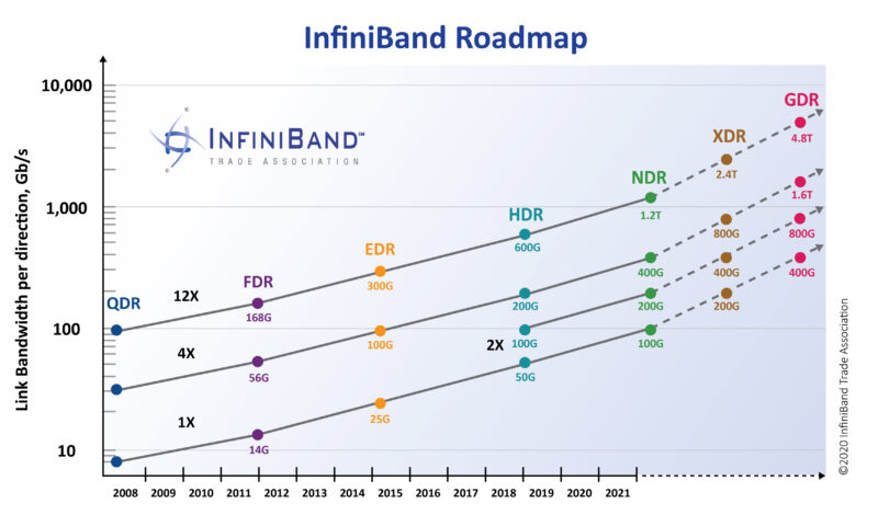
For bandwidth between nodes across a supercomputer, you can look for instance at InfiniBand’s roadmap. Again we see an exponential trend, that roughly keeps pace with transistor scaling.
There has also been a recent trend in ‘chiplet’ architectures, whereby multiple dies are connected together with short, dense, and efficient connections. This includes both 2D stacking, where the chips are placed side-by-side, with short and dense local traces connecting them, and 3D stacking, where the chips are placed on top of each other. 3D stacking allows for extremely high bandwidth connections, because the connections are so short and of great number, but currently needs to be done carefully to avoid heat concentration. This is an emerging technology, so again rather than showing any single trendline in capability scaling, I will list a few relevant data points.
Intel’s upcoming Ponte Vecchio supercomputer GPU connects 41 dies, some compute and some memory, using ‘embedded bridges’, which are small silicon connections between dies.
AMD’s already sampling MI200 server GPU also integrates two compute dies plus some memory dies in a similar fashion. Their Milan-X server CPUs will stack memory on top of the CPU dies to expand their local cache memory, and those dies are then connected to other CPU dies an older lower-performance interconnect.
Cerebras have a ‘wafer-scale engine’, which is a circuit printed on a wafer that is then used as a single huge computing device, rather than cut into individual devices.
Tesla have announced the Dojo AI supercomputer, which puts 25 dies onto a wafer in a 5x5 grid, and then connects those wafers to other wafers in another higher-level grid. Each die is connected directly only to its four nearest neighbors, and each wafer only to its four nearest neighbors.
2. There’s Plenty [more] Room at the Bottom
Richard Feynman gave a lecture in 1959, There’s Plenty of Room at the Bottom. It is a very good lecture, and I suggest you read it. It is the kind of dense but straightforward foresight I think rationalists should aspire to. He asks, what sort of things does physics allow us to do, and what should the techniques that get us there look like?
Feynman mentions DNA as an example highly compact dynamic storage mechanism that uses only a small number of atoms per bit.
This fact – that enormous amounts of information can be carried in an exceedingly small space – is, of course, well known to the biologists, and resolves the mystery which existed before we understood all this clearly, of how it could be that, in the tiniest cell, all of the information for the organization of a complex creature such as ourselves can be stored. All this information – whether we have brown eyes, or whether we think at all, or that in the embryo the jawbone should first develop with a little hole in the side so that later a nerve can grow through it – all this information is contained in a very tiny fraction of the cell in the form of long-chain DNA molecules in which approximately 50 atoms are used for one bit of information about the cell.
To ask for computers to reach 50 atoms per transistor, or per bit of storage, is a big ask. It’s possible, as DNA synthesis for storage is a demonstrated technology, and perhaps even useful, but for compute-constrained AI applications we are interested in high throughput, dynamic memories, presumably electronic in nature. Even if it might be possible to build useful and applicable systems with DNA or other molecular devices of that nature, it is not needed to assume it for this argument.
The overall impressions I expect to be taken from this section are that,
IRDS roadmaps already predict enough scaling for significant short-term growth.
3D stacking can unlock orders of magnitude of further effective scaling.
Memory has a large potential for growth.
Integrated systems for training can get very large.
Section note: Many of the numbers in this section are Fermi estimates, even when given to higher precision. Do not take them as precise.
How small could we go?
The IRDS roadmap mentioned at the start of this post suggests Moore’s Law device scaling should continue until around 2028, after which it predicts 3D integration will take over. That suggests a planar density of around 10⁹ transistors/mm². Already this planar density is much greater than today. NVIDIA’s most recent Ampere generation of GPUs has a density around 5×10⁷, varying a little depending on whether they use TSMC 7nm or Samsung 8nm. This means that a dumb extrapolation still predicts about a factor of 20 improvement in transistor density for GPUs.
Continuing to ignore scale-out, the industry is looking towards 3D integration of transistors. Let’s assume a stacked die has a minimal thickness of 40µm per layer. A 30×30×4 mm die built with 100 stacked logic layers would therefore support 100 trillion transistors. This is about 50 times greater than for a Cerebras CS-2, a wafer-scale AI accelerator. Having 100 logic layers could seem like a stretch, but Intel is already selling 144 layer NAND flash, so skyscraper-tall logic is far from provably intractable. AI workloads are extremely regular, and many require a lot of space dedicated to local memory, so variants of existing vertical scaling techniques might well be economical if tweaked appropriately.
This answer, while promising much of room for future device scaling, is still not physically optimistic. A device of that size contains 2×10²³ silicon atoms, so it has a transistor density of around one transistor per 2×10⁹ atoms. Using transistors for dynamic storage (SRAM) would increase that inefficiency by another factor ~5, since individual transistors are transient, so this hypothetical device is still about a factor of 10⁸ less atomically efficient than DNA for storage.
At a density of 10⁹ transistors/mm², if perfectly square, our assumed 2028 transistor operates a footprint about 120×120 atoms across. If you could implement a transistor in a box of that dimension on all sides, with only a factor ~10 in overheads for wiring and power on average, then each transistor would require only 2×10⁷ atoms, a factor of 100 improvement over the previous number. It is unclear what specific technologies would be used to realize a device like this, if it is practically reachable, but biology proves at least that small physical and chemical switches are possible, and we have only assumed exceeding our 2028 transistor along one dimension.
Although this device is stacked only modestly relative to the brain, power density does at some point become an issue beyond the capabilities of current methods. Heat density is easily handled with integrated cooling channels, provided enough cool liquid, which is a demonstrated technology. Total rack power output might have some fundamental limits somewhere eventually, but the ocean makes a good heatsink. So I don’t believe that cooling represents a physical barrier.
How much can we improve on DRAM?
Per earlier in this writeup, DRAM scaling has hit a bottleneck. Not every AI accelerator uses DRAM as their primary storage, with some relying on faster, more local SRAM memory, which is made directly from transistors arranged in an active two-state circuit.
As of today, and for a long time prior, DRAM is an optimal balance of speed and density for large but dynamically accessed memory. DRAM is fast because it is made of transistor-gated electric charges, and is more space efficient than SRAM by virtue of its simplicity.
The complexity of an SRAM cell is a consequence of transistors being volatile, in that they don’t retain state if their inputs subside. You therefore need to build a circuit that feeds the state of the SRAM memory back into the inputs of the SRAM memory, while also allowing that state to be overridden. What is important to note is that this is a statement of CMOS transistors, not a statement about all switches in general. Any device that can hold two or more states that can be read and changed electrically holds promise as a memory storage.
Memory has more relaxed requirements than transistors with regards to speed and switching energy, because typically only a little memory is accessed at a time. This is especially true for large scale network training, as each neural network weight can be reused in multiple calculations without multiple reads from bulk memory.
The problem with predictions of the future in a space like this is not that there are no clear right answers, as much as that there are so many prospective candidates with slightly different trade-offs, and correctly evaluating each one requires an immense understanding of its complicated relationship to the most complicated manufacturing processes on the planet. Therefore I will illustrate my point by choosing an example prospective technology that I think is neat, not by claiming that this particular technology will pan out, or be the best example I could have used. The space of technologies is so vast, the need is so great, and the history of memory technologies so demonstrably flexible, that it is all but inevitable that some technology will replace DRAM. The relevant questions to us are with regards to the limiting factors for memory technologies of these sorts in general.
NRAM is my simple to illustrate example. An NRAM cell contains a slurry of carbon nanotubes. Those carbon nanotubes can be electrically forced together, closing the switch, or apart, opening it.
Nantero claim they expect to reach a density of 640 megabits/mm² per layer on a 7nm process, with the ability to scale past the 5nm process. They also claim to support cost-effective 3D scaling, illustrating up to 8 process layers and 16 die stacks (for 128 total layers). This compares to 315 megabits/mm² for Micron’s upcoming 1α DRAM, or to ~1000 megatransistors/mm² for our projected 2028 logic node.
NRAM is a bulk process, in that many carbon nanotubes are placed down stochastically. This makes placement easy, but means we are still far from talking about physical limits. This is fine, though. The 128 layer device mentioned above would already have a bit density of 10 GB/mm². If you were to stack one die of 8 layers on top of a Cerebras CS-2, it would provide 240 terabytes of memory. This compares favourably to CS-2′s 40 gigabytes of SRAM.
Again, this is not to say that that this particular technology or device will happen. Most prospective technologies fail, even the ones I think are cool. I am saying that physics allows you to do things like this, and the industry is trying very many paths that point this way.
How big could we go?
When I initially envisioned writing this section, I had to justify the feasibility of large nearest-neighbor grids of compute, extrapolating from other trends and referencing interconnect speeds. Tesla made things easy for me by announcing a supercomputer that did just that.
Tesla starts like several other AI accelerators with a small compute unit that they replicate in a grid across the die, what they call their D1 chip. D1 is 645 mm² and contains 354 such units. They claim it’s 362 TFLOPS BF16/CFP8, which compares reasonably against the 312 TFLOPS BF16 from NVIDIA’s A100′s neural accelerator. (The A100 is a bigger 826 mm² die, but most of that space is dedicated to other GPU functionality.)
This compute unit is surrounded by densely packed, single-purpose IO, with a bandwidth of 4 TB/s in each ordinal direction, or 12 TB/s overall. This is a lot, considering an A100 has only 0.6 TB/s total bandwidth over NVLink, and 1.6 TB/s bandwidth to memory. For this bandwidth to be achieved, these chips are placed on a wafer backplane, called Integrated Fan Out System on Wafer, or InFO_SoW. They place a 5x5 grid, so 16,125 mm² of wafer in total, about a third the area of Cerebras’ monolithic wafer-scale accelerator, and they call this a ‘tile’.
Whichever approach up to that point is superior, Tesla’s tile or Cerebras’ waffle, the key scale difference happens when you connect many of these together. Tesla’s wafers have 9 TB/s of off-chip bandwidth in each ordinal direction, or 36 TB/s total bandwidth. This allows connecting an almost arbitrary quantity of them together, each communicating with their nearest neighbors. They connect 120 of these tiles together.
The topology of those 120 tiles is unclear, but for matters of theory we can assume what we want. If the arrangement is a uniform 12x10 grid, then a bisection along the thinnest axis would have a total bandwidth of 90 TB/s. That is quite fast!
Although bandwidth is high, you might start to be concerned about latency. However, consider pipeline parallelism, splitting different layers of the graph across the nodes. GPT-3 has 96 attention layers, so at that scale each layer corresponds to ~1 tile. Information only needs to rapidly pass from one tile to its neighbor. Latency is unlikely to be a concern at that scale.
Now consider a huge computer with, say, 100 times the number of tiles, each tile being significantly larger according to some growth estimates, running a model 1000 times as large as GPT-3. This model might have only 10 times the number of layers, so you might need ten tiles to compute a single layer. Still, a model partition does not seem bound by fundamental latency limits; 10 tiles is still spatially small, perhaps a 3x3 grid, or perhaps even a 3D arrangement like 2x2x3.
If these tiles have excess memory, as the NRAM example in the previous subsection showed is physically realizable, you can make the problem even simpler by replicating weights across the local tiles.
Ultimately, the sort of AI training we do now is very conducive to this sort of locality. Cerebras already has to grapple with compiling to this architecture, just on their one wafer-scale chip.
Even if more point-to-point data movement is needed, that is far from infeasible. Optical interconnects can carry extremely high physically realizable bandwidths over long distances, with latency limited to the speed of light in fibre plus endpoint overheads. Ayar Labs offers TerraPHY, which is a chiplet (a small add-on chip) that supports 2 Tb/s per chiplet and a maximum length of 2km. Even that longest version would purportedly have a latency of just 10 µs, dominated by the speed of light. If every layer in a 1000 layer network had a 10 µs communication latency added to it that wasn’t pipelined or hidden by any other work, the total latency added to the network would be 10 ms. Again, physics doesn’t seem to be the limiting factor.
3. How much die could a rich man buy?
One of the many insights Feynman got right in There’s Plenty of Room at the Bottom is that shrinking the size of things would make them proportionally more mass manufacturable, and similarly, proportionally cheaper. However, in much of this essay I have talked about scaling upwards: more layers, more devices, bigger systems, bigger prices. It is natural to wonder how much of this scaling up can be done economically.
In this section I want to argue for expecting the potential for significant economic scaling beyond Moore’s Law, both in terms of lower prices and in terms of higher spending. I do not put a timeline on these expectations.
The overall impressions I expect to be taken from this section are that,
There exist plausible prospective technologies for making fabrication cheaper.
Funding could scale, and that scale could buy a lot more compute than we are used to.
You can make things pretty cheap, in theory
Semiconductors are the most intrinsically complex things people manufacture, and it’s hard to think of a runner up. The production of a single chip takes 20+ weeks start to end, and a lot of that work is atomically precise. Just the lightbulbs used to illuminate wafers for photolithography steps are immensely complex, bus-sized devices that cost upwards of $100m each. They work by shooting tiny droplets of tin, and precisely hitting those with a laser to generate exactly the right frequency of light, then cascading this through a near atomically exact configuration of optics to maximize uniformity. Actually, the droplets of tin are hit twice, the first pulse creating a plume that more efficiently converts the energy of the second laser into the requisite light. And actually, some of the mirrors involved have root mean square deviations that are sub-atomic.
Semiconductor manufacturing is hard, and this makes it expensive. It is, honestly, fairly miraculous that economies of scale have made devices as cheap as they are.
On the other hand, atomic manufacturing, even atomically precise manufacturing, is normally practically free. Biology is almost nothing but great quantities of nanomachines making nanoscale structures on such a scale that sometimes they produce giant macroscopic objects. It is not physics that is telling us to make things in expensive ways.
For all the cutting edge of semiconductor manufacturing is pricey, some of the less exacting stuff is pretty affordable per square millimetre. TV screens can be massive, but are covered in detailed circuitry. Typically this discrepancy is down to a simpler method of construction. Often inkjet printing is used—literally a printer that deposits droplets of the desired substance on the flat backplane, printing out the wanted circuitry.
These methods have limitations. Inkjet printers are not very precise by photolithography standards, and can be rate limited for complex designs. Semiconductor manufacturing tends to involve several slower steps, like atomic vapor deposition, to place down layers one atom thick at a time, and etching steps for more complex 3D constructions. Sometimes layers are ground flat, to facilitate further build up of material on top of that. These steps make the difference between the price per square millimetre of CPU, and the price per square millimetre of TV. If you could use the latter production techniques to build high end CPUs, we’d be doing it already.
Biology does still inspire us to ask what the practically achievable improvements to manufacturing speed and affordability are. There are a couple of innovative techniques I know of that do scale to promising resolutions, and are under research. Both are stamping methods.
Nanoimprint lithography works by stamping an inverse of the wanted pattern into a soft solid, or a curable liquid, to form patterns.
Nanoscale offset printing uses, in effect, an inked stamp of the pattern to transfer, copying it from a master wafer to the target.
Both techniques allow bulk copies of complex designs in much shorter periods of time, with orders of magnitude less capital investment. Nanoimprint lithography is harder to scale to high throughput, but has comparable resolution to the best photolithography tools. Nanoscale offset printing is quick to scale, but likely has some fundamental resolution limits just shy of the best photolithography techniques.
I don’t want to go too much into the promise of these and other techniques, because unlike prospective memory technologies, there aren’t an effective infinity of choices, and these ideas may very well not pan out. My goal in this section is to raise the legitimate possibility that these economic advances do eventually happen, that they are physically plausible, if not promised, and to get people to ponder on what the economic limits to scale would be if, say, semiconductors fell to around the price per unit area of TVs.
You can spend a lot more money, in theory
Governments don’t have the best foresight, but they do like spending money on things. The Space Launch System, NASA’s new space rocket, is projected to cost >$4B per launch in running costs, and between the launch vehicle, the capsule, and the ground equipment, well over $40B has been spent on it to date. The government could bankroll huge AI projects.
Several particularly rich people have more foresight (or just more gutzpah) than the government, while also having a better ability to spend their large quantities of money efficiently. Elon Musk has a huge amount of money, around $300B, an uncommon belief in AI progress, and the willingness to spend large numbers of billions on his passion projects. Elon Musk could bankroll huge AI projects.
Investments of this scale are not outside of traditional industry, if revenue sources exist to justify it. TSMC is investing $100 billion over three years in expanding semiconductor manufacturing capacity. NVIDIA’s meteoric stock rise and Softbank’s $100B Vision Fund’s AI focus shows industry is betting on AI to have large returns on investment. I don’t know where I predict things to land in the end, but it does not seem wise to assume investments of this sort cannot flow down into models, should they show sufficiently impressive capabilities.
So, let’s modestly say $10B was invested in training a model. How much would that buy? A cutting edge semiconductor wafer is around $20,000, excluding other component costs. If $2B of the overhead was just buying wafers, that buys you about 100,000 wafers, or about half a month of capacity from a $12B 5nm fab. The other components are pricey enough to plausibly take up the remainder of the $10B total cost.
100,000 wafers translates to 100,000 Cerebras wafer-scale devices. For context, the Aurora supercomputer is estimated to cost $500m, or ¹⁄₂₀th of the cost, and would have ~50,000 GPUs, each a large device with many integrated chiplets, plus stacked memory, and plus CPUs. The numbers seem close enough to justify running with that number. Individual Cerebras machines are much more expensive than our estimate of ~$100k each (of which 10% is the wafer cost), but the overheads there are likely due to low volumes.
Cerebras talks about the feasibility of training 100 trillion parameter models with factor-10 sparsity on a cluster of 1000 nodes in one year. Our modest example buys a supercomputer 100 times larger. There is also no requirement in this hypothetical to assume that we are purchasing today’s technology, today. Scaling to very large supercomputer sizes seems feasible.
4. And I would think 1,000 miles
Prior to this section, I have tried to walk a fine line between bold claims and ultraconservatism. I want to end instead with a shorter note on something that frames my thinking about scaling in general.
So far I have talked about our artificial neural networks, and their scaling properties. These are not the ultimate ground limits. We know, at minimum, that brains implement AGI, and to the best of my knowledge, here are some other things that seem quite likely.
The bulk of signalling happens through chemical potential neuron spikes.
Neurons can fire at about 250-1000 Hz when active.
On average across the brain, neurons fire at 0.2 Hz.
Its density in humans is about 10⁸ neurons/mm³.
At ~1B/synapse and 100T synapses, the brain has ~100TB storage.
Contrast silicon,
The bulk of signalling happens through switching voltages in wires.
Isolated transistor speeds are in excess of 200 GHz.
Active (“hot”) transistors usefully switch at around 1-5 GHz on average.
Density is around 10⁸ transistors/mm²—that’s areal density, not volumetric.
You can buy an 8TB SSD off Amazon for ~$1000.
If we assume two iPhones floating in space were simulating two connected neurons, with direct laser links between them, in order for the two to communicate with worse than the ~1/200 second latency as neighboring neurons in our brains do, either,
The two phones would need to be over 1000 miles away from each other, about the radius of the moon.
The phones would have to be doing a calculation with a sequential length of 10⁷ clock cycles, if running on the CPU cores, which if I recall correctly can together do something like 30 independent operations per cycle.
Thus, for the silicon advantage to start hitting scale out limits relative to what we know is biologically necessary, we would need to be building computers about the size of the moon.
(I also worry a bit about quantum computers. Some of this is perhaps just that I don’t understand them. I think a lot of it is because they expand the space of algorithms drastically beyond anything we’ve seen in nature, those algorithms seem relevant for search, and Neven’s Law means any new capabilities that quantum computers unlock are likely to come suddenly. I think people should pay more attention to quantum computers, especially now that we are at a transition point seeing regular claims of quantum supremacy. Quantum computers can do computational things that no other known process has done ever.)
This, in my mind, is ultimately why I am so hesitant to believe claims of physical limits impeding progress. We are not that many orders of magnitude away from how small we can build components. We are sometimes starting to fight certain physical limits of information transfer through certain electromagnetic signals through limited space. In places we are even hitting practical questions of costs and manufacturing. But we are not building computers the size of the moon. Physics is a long, long, long way away from telling us to pack up, that there’s nothing left to do, that AI systems cannot grow bigger before they stop being suitable for building AI. The limits we are left with are limits of practice and limits of insight.
End note: In retrospect, there are two things I should have addressed that I did not. One is energy efficiency, which ended up being discussed in the comments, and is important to understand. Another was photonic computing, particularly using photonics for matrix multiplication, which I am undecided about. Lightelligence and Lightmatter are two example startups in this space.
- The pace of progress, 4 years later by (29 Dec 2025 4:16 UTC; 25 points)
- 's comment on Lizka’s Quick takes by (EA Forum; 31 Aug 2025 15:44 UTC; 6 points)
- 's comment on Are we in an AI overhang? by (11 Dec 2021 17:15 UTC; 4 points)
- 's comment on Are we in an AI overhang? by (11 Dec 2021 17:15 UTC; 4 points)
I showed this article to Peter Glaskowsky, who has had a long career in chip design and works on AI chips now and, in addition to liking this article, he mentioned he considers your estimates to be a lower bound.
Re: quantum computing.
I am bearish it will be a big deal in relation to AI.
This is because:
The exponential speedups are very hard to achieve in practice.
The quadratic speedups are mostly lost when you parallelize.
At the current rate of progress and barring a breakthrough it seems it will be a couple of decades until we have useful quantum computing.
Huh. How much stock do you put in extrapolating trends in qubit count like that last link? I would assume that the tradeoff they see between chip size and quality is because of selection / publication bias, not manufacturing process per se. This means that once the un-selected manufacturing process can make error-corrected circuits, there’s capacity for a steep rise in investment and circuit size.
I do believe that the tradeoff is real, and has a very clear physical reason—larger chips require more gates to perform a single quantum operation, so if the topology of the chip is roughly the same then I expect the fidelity needed to prevent errors to increase drastically with size.
In any case, note that in the extrapolation we basically assumed that the tradeoff didn’t exist, so I expect the predictions to be pessimistic.
A larger question is whether these kind of historical extrapolations work at all. In fact, a large part of why I wrote this paper is precisely because I want to test this.
On this I am cautiously optimistic for hard-to-verbalize reasons.
I think the most legible reason is that technological discontinuities are somewhat rare in practice.
The hard-to-verbalize reasons are… points at the whole Eliezer vs OpenPhil and Christiano debate.
Did you mean bearish?
I keep making this mistake facepalm
Well done!
What do you think about energy costs? Last I thought about this it seemed plausible to me that in ten years or so the atoms making up supercomputers will be <10% of the cost of training giant models, most of the cost being paying for the electricity and upkeep and rent.
Lifetime energy costs are already significant, but I don’t think the problem will get that skew this decade. IRDS’ predicted transistor scaling until ~2028 should prevent power density increasing by too much.
Longer-term this does become a greater concern. I can’t say I have particularly wise predictions here. There are ways to get more energy efficiency by spending more on lower-clocked hardware, or by using a larger memory:compute ratio, and there are also hardware architectures with plausible significant power advantages. There are even potential ways for energy to fall in price, like with solar PV or fusion, though I haven’t a good idea how far PV prices could fall, and for fusion it seems like a roll of the dice what the price will be.
It’s entirely possible energy does just become the dominant cost and none of those previous points matter, but it’s also an input we know we can scale up pretty much arbitrarily if we’re willing to spend the money. It’s also something that only starts to become a fundamental economic roadblock after a lot more scaling. For instance, the 100,000 wafer scale processor example requires a lot of power, but only about as much as largest PV installations that currently exist. You could then upgrade it to 2028 technology and stack memory on top of the wafers without changing power density by all that much.
This is likely a topic worth periodically revisiting as the issue gets closer.
Ok, thanks! I defer to your judgment on this, you clearly know way more than me. Oh well, there goes one of my hopes for the price of compute reaching a floor.
As far as I understand, we’re only 3 orders of magnitude away from Landauer limit, which doesn’t leave a lot of room to squeeze efficiency out of. On the supply side, fusion doesn’t seem like a relevant factor before 2050 unless an alternative approach takes us by surprise. Solar PV efficiency is already on the OOM of 1, so any advances have to come from reduction in production and maintenance costs (which is plausible for all I know).
The Landauer limit constrains irreversible computing, not computing in general.
On the technology readiness level, I put reversible computing somewhere between von Neumann probes and warp drive. Definitely post-Singularity, likely impossible.
Knowing little about irreversible computing this nevertheless sound surprising to me. Why exactly is irreversible computing so hard?
EDIT ofc I meant reversible not irreversible computing here!
Irreversible is normal computing, the operation makes a state change which does not allow you to go backwards. Reversible computing is a lab curiosity at very small scale, using circuits which slide between states without dissipating energy and can slide the other way too. As Maxim says, it is far-out speculation whether we can really build computers that way.
Warp drive is more likely than not physically impossible, and even if possible would require insane energies, manipulating spacetime using exotic matter (which has never been produced) etc. It is a true magitech.
Von Neumann Probes seem easier; they re probably physically possible but the sheer engineering for it to work seems very very difficult. In fact there are no credible plans or ideas to even build one. Just having interstellar space travel is an immense task.
Doing thing with circuits seems comparatively more feasible.
Agreed. I had [this recent paper](https://ieeexplore.ieee.org/abstract/document/9325353) in mind when I raised the question.
I don’t expect a sustained Moore’s Law type improvement to efficiency here, just the possibility of a few technology jumps with modest but meaningful gains. A factor of 10 beyond CMOS would amount to an extension of a decade.
I probably have much shorter average fusion timelines than you, albeit also with high variance, and wouldn’t be hugely surprised if fusion ramped up commercial operations through the 2030s, nor would I be shocked if it didn’t. The new wave of fusion startups seem to have coherent justifications to me, as a layman.
I would be shocked if fusion provides >10% of electricity to any major economy in the 2030s, like cold-fusion-is-possible-level shocked. On the one hand, the technologies new fusion start-ups are working with are obviously much more plausible than cold fusion, on the other hand there are a LOT of likely ways for fusion to fail besides just technical problems, so my intuition tells me it’s a toss-up.
I don’t know nearly as much about solar PV so my confidence intervals there are much wider. I agree that if there was sufficient economic incentive, we could scale to incredible amounts of compute right now, crypto mining shows an empirical lower bound to that ability.
I agree with all of this. I wasn’t intending to imply fusion would lower global average prices in that timeframe. A massive supercomputer effort like I was describing could build its own plant locally if necessary.
My first and second impression on reading this is I want to bet against you, but I’m not even quite clear on what specific bet you are taking against Jensen/IRS/myself when you say:
Because you are hedging bets there, and then also here:
So what I’m wondering is what is your more exact distribution over Moore’s Law? To be specific, what is your distribution over the future graph of ops/$ or ops/J, such that it even disagrees with the mainstream (Jensen/IRS/myself/etc)?
To hold myself to that same standard, I predict that for standard available GPUs/TPUs/etc (irreversible parallel von-neumann machines), about 65% chance we can squeeze about 10x more ops/J out by 2028 (Moravec’s prediction of AGI), and only about a 10% chance we can squeeze out about 100x more ops/J.
Do you disagree? I believe ops/$ will be mostly dominated by ops/J.
The wildcard is neuromorphic computing, which can allow somewhat better-than brain (say 10x) or so noisy analog ops/J. But that’s a separate discussion, and those chips won’t run current DL well, they are mostly only good for more explicitly brain-like AGI.
2028 is 6 years and change away. Even a straight-line extrapolation of transistor density wouldn’t quite make a 10x improvement versus today’s cutting edge, and that scales better than switches-per-joule. So if we’re ignoring the device architecture, I think I’m more pessimal than you!
I don’t address ops/J in the article, though I respond to the question here. It seems totally reasonable to me that compute is eventually limited by energy production. At the same time, we are not currently anywhere near the limits of how much power we could feasibly pump into (or extract from) any one given supercomputer, and at minimum we have some power scaling left to expect from the roadmap.
You’re right to call out the hedging in my article, but it is legitimate uncertainty. I expect progress to about match IRDS until 2028, but predictions have been wrong, and I didn’t want people to take Moore’s Law’s seeming historic inviolability as evidence that it actually is inviolable.
To try to clarify and enumerate the relevant stances from the article,
The reports of Moore’s Law’s death have been greatly exaggerated, as it applies to current and historical trends.
I expect business as usual until at least around when the IRDS stops doing so, aka. 2028, after which IRDS expects scaling to come from 3D stacking of transistors.
AI performance will grow about proportionally to the product of transistor density and frequency, notwithstanding major computer architecture changes.
Some memory technology will displace traditional DRAM, likely this decade, with much better scaling properties. Plausibly several will.
You will see other forms of scaling, like 3D integration, continually make progress, though I’m not staking a claim on any given exponential rate.
Scaling up will happen proportionally to the money spent on compute, in the sense that we will not reach the point where we are physics limited, rather than resource limited, in how big AI systems can be.
I give some examples of feasible systems much larger and more capable than today’s.
If any of these don’t match what you got from the article, please point it out and I’ll try to fix the discrepancy.
Ok that might be a crux. I am claiming that new GPU designs are already energy limited; that is the main constraint GPU engineers care about.
I will update my off-the-cuff prediction with something more calibrated for posterity (that was an initial zero-effort guess), but I’m not ignoring device architecture. For the 2028 timeframe it’s more like only ~2x op/J increase from semiconductor process (when measuring say transistor flips/J), and ~5x op/J from low level architecture improvement in low-precision matrix multiply units (or say ~5x and ~20x for my lower prob estimate). I’m specifically talking about GPU/TPU style processors, not neuromorphic, as described earlier. (In part because I believe GPU/TPU will take us to AGI before neuromorphic matters) Much more of the pre-neuromorphic gain will come from software.
I believe 1.) is actually easy-to-estimate from physics, I’ve read said physics/ECE papers outlining the exact end of moore’s law, and I’m assuming Jensen-et-al has as well (and has deeper inside knowledge). The main constraint is more transit energy than transistor flip energy.
2.) Doesn’t actually extend Moore’s Law (at least by the useful definitions I’m using)
3.) GPUs aren’t limited by transistor count, they are limited by power—ie we are already well into ‘Dark Silicon’ era.
4.) This is already priced in, and doesn’t help enough.
5.) Doesn’t help logic enough because of power/heat issues, but it’s already important and priced in for RAM (eg HBM).
6.) I mean that’s an independent scaling axis—you can always spend more on compute, and we probably have more OOM of slack there? Orthogonal to the Moore’s Law predictions
7.) I’ll reply to those feasible system examples separately after looking more closely.
I agree this seems to be our main departure.
You seem to be conflating two limits, power limits, as in how much energy we can put into a system, and thermal limits, as in how much energy can we extract from that system to cool it down.
With regards to thermal limits, GPUs run fairly far into the diminishing returns of their power-performance curve, and pushing them further, even with liquid nitrogen, doesn’t help by a disproportionate amount. NVIDIA is pushing significantly more power into their top end GPUs than they need to approximately hit their peak performance. Compare phone to laptop to desktop GPUs; efficiency/transistor improves drastically as power goes down. So it seems to me like GPUs are not yet thermally limited, in the sense that having more transistor density would still allow performance scaling even in lieu of those transistors becoming more efficient.
Arguably this could be a result of architectural trade-offs prioritizing mobile, but flagships sell cards, and so if NVIDIA was willing to give those cards so much power, they should optimize for them to consume that much power. I’d also expect that to pan out as a greater advantage for competitors that target servers specifically, which we don’t see. Anyhow, this isn’t a physical limit, as there exist much better ways to extract heat than we are currently using, if this was something that scaling needed doing.
You seem mostly concerned on the other point, which is the power limit, specifically those derived from the price for that power. My understanding is that power is a significant fraction of server costs, but still significantly less than the amortized cost of the hardware.
I didn’t use the word thermal, but of course they are trivially related as power in = heat out for irreversible computers, so power/thermal limit can be used interchangeably in that sense. GPUs (and any processor really) have a power/thermal design limit based on what’s commercially feasible to support both in terms of the power supply and the required cooling.
This doesn’t make sense to me—in what sense are they not thermally limited? Nvidia could not viably put out a consumer GPU that used 3 kilowatts for example. The RTX 3090 pushing power draw up to 350 watts was a big deal. Enterprise GPUs are even more power constrained, if anything (the flagship A100 uses 250 watts—although I believe it’s using a slightly better TSMC node rather than samsung) - and also enormously more expensive per flop.
A 2x density scaling without a 2x energy efficiency scaling just results in 2x higher dark silicon ratio—this is already the case and why nvidia’s recent GPU dies are increasingly split into specialized components: FP/int, tensorcore, ray tracing, etc.
I’m not sure what you mean here—from what I recall the flip/J metrics of the low power/mobile process nodes are on the order of 25% gains or so, not 100%. Phones/laptops have smaller processor dies and more dark silicon, not dramatically more efficient transistors.
That naturally depends on the age of the hardware—eventually it will become useless when it’s power + maintenance cost (which is also mostly power/thermal driven) exceeds value.
For example—for a 3090 right now the base mining value (and thus market rate) is about $8/day, for about $1/day of electricity (at $0.15 / kwhr) + $1/day for cooling (1:1 is a reasonable rule of thumb, but obviously depends on environment), so power/thermal is about 25% vs say 10% discount rate and 65% depreciation. Whereas it’s more 50⁄50 for an older 1080 ti.
Power in = power out, but a power limit is quite different to a thermal limit. An embedded microcontroller running off a watch battery still obeys power in = power out, but is generally only limited by how much power you can put in, not its thermals.
This is the wrong angle to look at this question. Efficiency is a curve. At the point desktop GPUs sit at, large changes to power result in much smaller changes to performance. Doubling the power into a top end desktop GPU would not increase its performance by anywhere near double, and similarly halving the power only marginally reduces the performance.
It is true that devices are thermally limited in the sense that they could run faster if they had more power, but because of the steep efficiency curve, this is not at all the same as saying that they could not productively use more transistors, nor does it directly corresponds to dark silicon in a meaningful way. The power level is a balance between this performance increase and the cost of the power draw (which includes things like the cost of the power supplies and heatsink). As the slope of power needed per unit extra performance effectively approaches infinity, you will always find that the optimal trade-off is below theoretical peak performance.
If you add more transistors without improving those transistors’ power efficiency, and without improving power extraction, you can initially just run those greater number of transistors at a more optimal power ratio.
This is not true. GPUs can run shader cores and RT cores at the same time, for example. The reason for dedicated hardware for AI and ray tracing is that dedicated hardware is significantly more efficient (both per transistor and per watt) at doing those tasks.
The point isn’t the logic cell, those tend to be marginal improvements as you say. The point is that those products are operating at a much more efficient point on the power-performance curve. Laptop NVIDIA GPUs are identical dies to their desktop dies (though not always to the same model number; a 3080 Mobile is a desktop 3070 Ti, not a desktop 3080). Phone GPUs are much more efficient again than laptop GPUs.
It is true that a phone SoC has more dark silicon than a dedicated GPU, but this is just because phone SoCs do a lot of disparate tasks, which are individually optimized for. Their GPUs are not particularly more dark than other GPUs, and GPUs in general are not particularly more dark than necessary for their construction.
It should also be noted that dark silicon is not the same as wasted silicon.
Note that Google claims ~10:1.
I’m not convinced mining is a good proxy here, their market is weird, but it sounds like you agree that power is a significant but lesser cost.
Are you talking about clock rates? Those haven’t changed for GPUs in a while, I’m assuming they will remain essentially fixed. Doubling the power into a desktop GPU at fixed clock rate (and ignoring dark silicon fraction) thus corresponds to doubling the transistor count (at the same transistor energy efficiency), which would double performance, power, and thermal draw all together.
Jensen explicitly mentioned dark silicon as motivator in some presentation about the new separate FP/int paths in ampere, and I’m assuming the same probably applies at some level internally for the many paths inside tensorcores and RT cores. I am less certain about perf/power for simultaneously maxing tensorcores+RTcores+alucores+mempaths, but I’m guessing it would thermal limit and underclock to some degree.
Primarily through lowered clock rates or dark silicon. I ignored clock rates because they seem irrelevant for the future of Moore’s law.
Google has unusually efficient data-centers, but I’d also bet that efficiency measure isn’t for a pure GPU datacenter, which would have dramatically higher energy density and thus cooling challenges than their typical light CPU heavy storage search-optimized servers.
Clock rate is relevant. Or rather, the underlying aspects that in part determine clock rate are relevant. It is true that doubling transistor density while holding all else equal would require much more thermal output, but it’s not the only option, were thermal constraints the dominant factor.
I agree there is only so much room to be gained here, which would quickly vanish in the face of exponential trends, but this part of our debate came up in the context of whether current GPUs are already past this point. I claim they aren’t, and that being so far past the point of maximal energy efficiency is evidence of it.
This doesn’t make sense technically; if anything Ampere moves in the opposite direction, by making both datapaths be able to do FP simultaneously (though this is ultimately a mild effect that isn’t really relevant). To quote the GA102 whitepaper,
I briefly looked for the source for your comment and didn’t find it.
We are interested in the compute frontier, so this is still relevant. I don’t share the intuition that higher energy density would make cooling massively less efficient.
I was aware the 3090 had 2x FP32, but I thought that dual FP thing was specific to the GA102. Actually the GA102 just has 2x the ALU cores per SM vs the GA100.
There are efficiency transitions from passive to active, air to liquid, etc, that all depend on energy density.
This topic is interesting because perception of Moore’s law varies a lot depending on whether you’re looking at production or R&D. In terms of R&D, manufacturers are already testing the limits of silicon (and so of course Moore’s law is already a dead law walking) - the 2028 timeline is just how long people expect it to take to roll out what we already have.
And by “roll out,” of course I mean “switch over to the entirely new designs and manufacturing techniques required to do anything useful with higher-precision lithography,” because everything is way more complicated than it was 20 years ago.
The average cortical neuron firing rate is much lower than this.[0] You might have meant maximum rather than average—or am I misunderstanding?
[0] https://aiimpacts.org/rate-of-neuron-firing/#:~:text=Based%20on%20the%20energy%20budget,around%200.16%20times%20per%20second.
I was indeed misremembering some statistic for which 200 Hz is correct, likely average peak rate or somesuch, not sure exactly. Thanks for catching this.
(Moderation note: added to the Alignment Forum from LessWrong.)
Nitpick: this would be more accurately described as pipeline parallelism; the term model parallelism is ambiguous since sometimes it’s used as an umbrella term for everything other than data parallelism, but it’s typically taken to mean splitting each layer across multiple nodes.
Fair clarification, I’ve edited the post.
Nice article. Good that you spotted the DRAM problem, many people don’t realize DRAM hit a scaling wall nearly 10 years ago. It has to do with the amount of charge needed to provide a sensible change at the end of the wires. As wires scale smaller their RC constant gets worse and competes with other factors that might improve, driving the capacitors to stay in the same range of total charge. Meanwhile the diameter of the capacitors is tough to change, with the minimum diameter set by material constants of dielectric and voltage breakdown. We found the best a while ago. The only way to pack the capacitors closer is to reduce the difference between the widest part of the cylinder and the minimum—which requires perfecting the aspect ratio and minimizing fluctuations. Slow, slow progress and when you reach perfection there remains that minimum diameter, rather like hitting the speed limit on transistors.
If you estimate the cost of a Graviton 2 core it comes out to about $5, but the 4GB of memory assigned to it cost about $12. You can do similar calculations for Apple M1 series. DRAM is already the cost limit, because it has for so long been the scaling laggard.
We will need new types of memory far more urgently than worrying about logic scaling.
Several more considerations which favour progress in computing:
Even if Moore’s law will stop, we could still produce more chips on existing fabs, and they will be much cheaper, as there will be no expenses on intellectual properties and no amortisation costs needed to develop better fabs and chips.
As the total size of the world economy is growing, relative price of a large computer is smaller.
Cloud computing allows researchers not to pay in advance for hardware which may or may not be effectively used.
Data centres are expensive, so smaller physical size of a computer is important as well as smaller energy consumption, even if it has the same price for flops. But larger data centres are more cost efficient.
Great post! I especially liked that you outlined potential emerging technologies and the economic considerations.
Having looked a bit into this when writing my TAI and Compute sequence, I agree with your main takeaways. In particular, I’d like to see more work on DRAM and the interconnect trends and potential emerging paradigms.
I’d be interested in you compute forecasts to inform TAI timelines. For example Cotra’s draft report assumes a doubling time of 2.5 years for the FLOPs/$ but acknowledges that this forecast could be easily improved by someone with more domain knowledge—that could be you.
I’m not all that sure this is going to give you anything more useful than what you have already. Around the end of this decade my compute predictions detach from any strict timeline, and the pace of progress within this decade is smaller than the potential range of money spent on the problem, so even if you draw a sure line around where TAI happens with today’s AI techniques, you don’t gain all that much from better guesses about hardware progress.
Put another way, if you assume current connectivist architectures scaled up to ~brain parity buys you most of the tools you need to build TAI, then you don’t need to worry about longer term hardware progress. If you don’t assume that, then you don’t have a meaningful anchor to use these longer term predictions with anyway. If I had strong timelines for physical technology progress you could at least say, architectures like P will be tried around the 20X0s, and architectures like Q will be tried around the 20Y0s, but I don’t have strong timelines for progress that goes that far out.
I do think understanding longer term tech progress is relevant, because I think that current AI systems do seem to keep buying relevant cognitive abilities as they scale, and having a long roadmap implies that we’ll keep doing that until the trick stops working or we hit AGI. But I don’t know how to put a date on that, at least one that’s more informative than ‘it’s technically plausible, and could come moderately soon if things go fast’.